Bilayer-induced asymmetric quantum Hall effect in epitaxial graphene
The magnetotransport properties of epitaxial graphene on SiC substrates play a central role in the development of monolithic technology for high quality graphene-based devices. Magnetotransport investigations in the quantum Hall regime provide valuable information on the disorder properties of the monolayer film and on the role of bilayer inclusions. In the quantum Hall regime, we show that bilayer stripes shunting the devices are responsible for anomalies in the observed characteristics, which we explain in terms of a Landauer-Büttiker model.
Recent years have seen the affirmation of scanning probe investigation techniques as powerful tools to investigate a great variety of transport phenomena in condensed matter physics. Among these techniques, scanning gate microscopy (SGM) has already been used to probe disorder potential, the properties of fractional and integer edge states in the quantum Hall regime, and for the spectroscopy of quantum dots. In SGM measurements, the conductive tip of an atomic force microscope is used to induce a local electrostatic perturbation of the device properties while recording the global response of the system.
Graphene is a very appealing candidate for SGM experiments, because it displays a high mobility and surface conduction, thus allowing operation of the SGM in very close proximity to the device. In particular, epitaxial growth of graphene on SiC is one of the routes pursued in the quest for monolithic integration of graphene, and has reached high mobility and uniformity on the wafer scale. In this form, graphene can be used for large scale fabrication of devices. Recently, the availability of a suitable dielectric made it possible to perform top-gating of the graphene layer, thus making SiC-based devices ideal for SGM experiments. In the following, we describe the development and characterization of graphene-based devices for SGM experiments aimed to achieve local control of the filling factor in the quantum Hall regime.
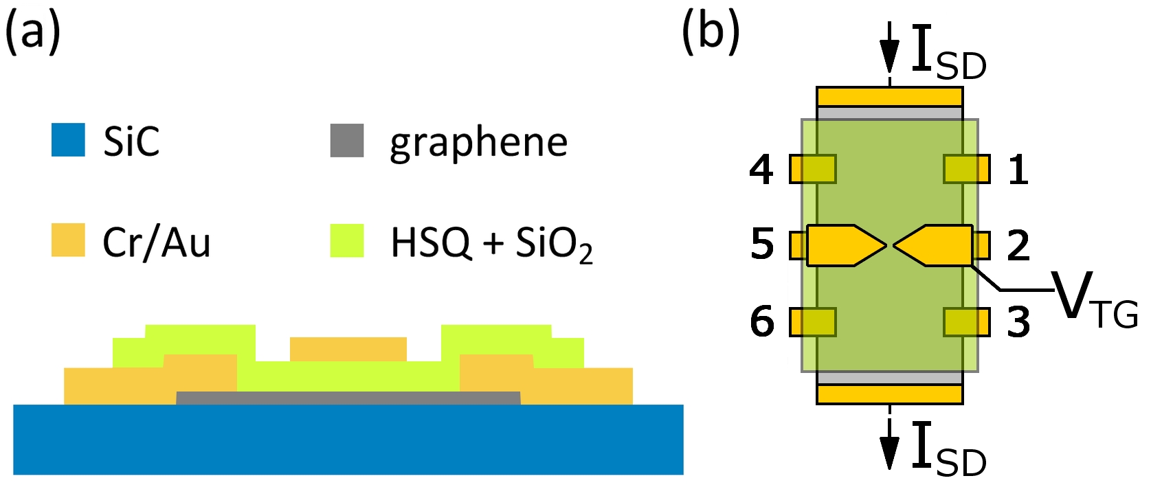 Fig. 1: (a) Cross-section and (b) layout of the device. The bilayer dielectric comprising Hydrogen Silsequioxane (HSQ) and SiO2 is shown as a single layer (green). The longitudinal and transversal resistances are acquired in a 4-point configuration at constant source-drain current ISD.
The device investigated in this work is a Hall-bar (length × width = 300 μm × 50 μm) fabricated by standard optical lithography from an epitaxial graphene layer grown on a 6H-SiC(0001) substrate. The epitaxial graphene was grown by annealing 6H-SiC(0001) in Ar atmosphere at 100 Torr. The annealing temperature was approximately 1820°C. A cross-section and a schematic of our device is displayed in Figs. 1(a) and (b), respectively. The orientation of the Hall-bar was deliberately chosen to be perpendicular to the SiC step edges, in order to have the terraces running across the device from one side to the other. Ohmic contacts were made by a Cr/Au (5/250 nm) metallic layer. As can be seen in Fig. 1(b), the ohmic contacts were not recessed as commonly done, but jutted out into the Hall-bar. A bilayer stack (140 nm of Hydrogen Silsequioxane (HSQ) and 40 nm of SiO2) was used as a dielectric. On top of this dielectric, Cr/Au (10/30 nm) electrodes in split-gate geometry were defined by e-beam lithography (not used in the experiments discussed here). We obtained similar results from another, nominally identical device.
The device design, shown in Fig. 1(b), is aimed at performing local tuning of the filling factor by the SGM tip. Measurements in the quantum Hall regime show a departure from the quantized resistance values expected for ideal monolayer graphene. In particular, at quantizing magnetic field, the longitudinal resistance assumes unexpectedly large values RXX≈10 kΩ, while the transversal resistance shows much lower values RXY≈2 kΩ. The most striking feature is that the magnetoresistance curves display peculiar symmetry properties, as shown in Figs. 2(a) and (b). Bilayer inclusions forming at the SiC atomic steps are believed to be responsible for the observed behavior. As supported by Raman maps of the device shown in Fig. 2(c), the step terraces of the SiC substrate were oriented perpendicularly to the Hall bar, and so long continuous bilayer stripes are present, which can cause shunting of the edge states at opposite sides of the bar. A simple model based on the Landauer-Büttiker formalism (see Fig. 2(d)) succeeds in explaining the observed transport anomalies.
 Fig. 2: Quantum Hall traces in a split-gate device containing graphene bilayer shunts: a) longitudinal and b) transversal resistance. c) Raman map of the device showing monolayer (light green) and bilayer (dark) graphene regions. The outline of the contacts and gates is superimposed. d) Schematic of edge state arrangement for a bilayer inclusion.
These measurements in the quantum Hall regime allow to shed light on the role of bilayer strips on the transport properties of epitaxial graphene on SiC, an aspect which is essential in the development of an effective integration technology.
Publications:
- Andrea Iagallo, Shinichi Tanabe, Stefano Roddaro, Makoto Takamura, Yoshiaki Sekine, Hiroki Hibino, Vaidotas Miseikis, Camilla Coletti, Vincenzo Piazza, Fabio Beltram, and Stefan Heun: Bilayer-induced asymmetric quantum Hall effect in epitaxial graphene, arXiv:1410.2024 [cond-mat.mes-hall].
- A. Iagallo, S. Tanabe, S. Roddaro, M. Takamura, Y. Sekine, H. Hibino, V. Miseikis, C. Coletti, V. Piazza, F. Beltram, and S. Heun: Bilayer-induced asymmetric quantum Hall effect in epitaxial graphene, Semicond. Sci. Technol. 30 (2015) 055007.
Presented at:
- Andrea Iagallo, Shinichi Tanabe, Stefano Roddaro, Makoto Takamura, Yoshiaki Sekine, Hiroki Hibino, Vaidotas Miseikis, Camilla Coletti, Vincenzo Piazza, Fabio Beltram, and Stefan Heun: Epitaxial Graphene Devices for Scanning Probe Measurements, SSDM 2014, Tsukuba, Japan, 8 – 11 September 2014 (oral). [Abstract] [Talk]
- S. Heun: 2D Materials Research Activities at the NEST lab in Pisa, Italy, NTT Basic Research Laboratories, Atsugi, Japan (Dr. S. Suzuki), 23 July 2015. [Abstract] [Talk]
- A. Iagallo, S. Tanabe, S. Roddaro, M. Takamura, Y. Sekine, H. Hibino, V. Miseikis, C. Coletti, V. Piazza, F. Beltram, and S. Heun: Bilayer-induced asymmetric quantum Hall effect in epitaxial graphene, EP2DS-21/MSS-17, Sendai, Japan, 26 – 31 July 2015 (poster). [Abstract] [Poster]