Black Phosphorus Planar Josephson Junctions
Setting up strong Josephson coupling in van der Waals materials in close proximity to superconductors offers several opportunities both to inspect fundamental physics and to develop cryogenic quantum technologies. Here we show evidence of Josephson coupling in a planar few-layer black Phosphorus junction. The planar geometry allows to probe the junction behavior by means of external gates, at different carrier concentrations. Clear signatures of Josephson coupling are demonstrated by measuring supercurrent flow through the junction at milli-Kelvin temperatures. Manifestation of Fraunhofer pattern with a transverse magnetic field is also observed, confirming the Josephson coupling. These findings represent evidence of proximity Josephson coupling in a planar junction based on a van der Waals material beyond graphene and will expedite further studies, exploiting the peculiar properties of exfoliated black phosphorus thin flakes.
Exfoliated black Phosphorus Surfaces investigated by Scanning Tunneling Microscopy
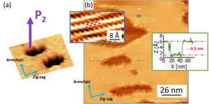
Black Phosphorus (bP) has emerged as an interesting addition to the category of two-dimensional materials. Surface-science studies on this material are of great interest, but they are hampered by bP’s high reactivity to oxygen and water, a major challenge to scanning tunneling microscopy (STM) experiments. As a consequence, the large majority of these studies were performed by cleaving a bulk crystal in situ. We have studied surface modifications on exfoliated bP flakes upon consecutive annealing steps, up to 550 C, well above the sublimation temperature of bP. In particular, our attention is focused on the temperature range 375 C – 400 C, when sublimation starts, and a controlled desorption from the surface occurs alongside with the formation of characteristic well-aligned craters. There is an open debate in the literature about the crystallographic orientation of these craters, whether they align along the zigzag or the armchair direction. Thanks to the atomic resolution provided by STM, we are able to identify the orientation of the craters with respect to the bP crystal: the long axis of the craters is aligned along the zigzag direction of bP. This allows us to solve the controversy, and, moreover, to provide insight in the underlying desorption mechanism leading to crater formation.
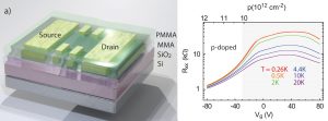
Ohmic contact engineering in few-layer black Phosphorus field effect transistors
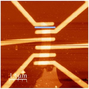
Achieving good quality Ohmic contacts to van der Waals materials is a challenge, since at the interface between metal and van der Waals material different conditions can occur, ranging from the presence of a large energy barrier between the two materials to the metallization of the layered material below the contacts. In black phosphorus (bP), a further challenge is its high reactivity to oxygen and moisture, since the presence of uncontrolled oxidation can substantially change the behavior of the contacts. Here we study three of the most commonly used metals as contacts to bP, chromium, titanium, and nickel, and investigate their influence on contact resistance against the variability between different flakes and different samples. Using the transfer length method, from an analysis of ten devices, both at room temperature and at low temperature, Ni results to provide the lowest contact resistance to bP and minimum scattering between different devices. Moreover, we observe that our best devices approach the quantum limit for contact resistance both for Ni and for Ti contacts.
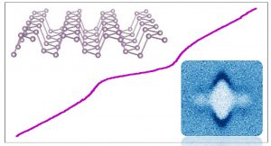
Phosphorene, a new two-dimensional platform for advanced materials
Two dimensional materials are still an unexplored territory. Graphene is one of the principal platform on which material scientists have only recently started to play. On the other side, it was estimated that a few hundreds of layered materials could be exfoliated to give a 2D crystal, allowing a large growing opportunity of research. Only small amounts of single and few layers sheets of Phosphorene, the all-P counterpart of graphene, have been prepared by exfoliation of black phosphorus, the most stable and least reactive of the allotropic forms of phosphorus, either by micromechanical cleavage (Scotch tape method) or liquid exfoliation. A phosphorene sheet has the same honeycomb hexagonal network of graphene but it is corrugated, since the P atoms have an sp3 hybridization. Phosphorene is a natural semiconductor, and the band gap can be controlled by changing the number of stacked layers. This makes the materials very promising for a wide variety of electronic applications.
Non-Classical Longitudinal Magneto-Resistance in Anisotropic Black Phosphorus
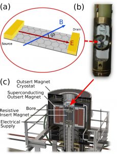
Resistivity measurements of a few-layer black phosphorus (bP) crystal in parallel magnetic fields up to 45 T are reported as a function of the angle between the in-plane field and the source-drain (S-D) axis of the device. The crystallographic directions of the bP crystal were determined by Raman spectroscopy, with the zigzag axis found within 5 deg of the S-D axis, and the armchair axis in the orthogonal planar direction. A transverse magneto-resistance (TMR) as well as a classically-forbidden longitudinal magneto-resistance (LMR) are observed. Both are found to be strongly anisotropic and non-monotonic with increasing in-plane field. Surprisingly, the relative magnitude (in %) of the positive LMR is larger than the TMR above 32 T. Considering the known anisotropy of bP whose zigzag and armchair effective masses differ by a factor of approximately seven, our experiment strongly suggests this LMR to be a consequence of the anisotropic Fermi surface of bP, as proposed theoretically in the context of three-dimensional structures [Pal and Maslov, Phys. Rev. B81, 214438 (2010)].
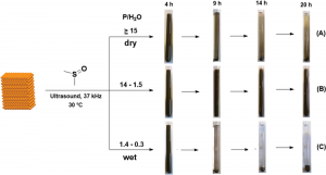
Hybrid Nanocomposites of 2D Black Phosphorus Nanosheets Encapsulated in PMMA Polymer Material: New Platforms for Advanced Device Fabrication
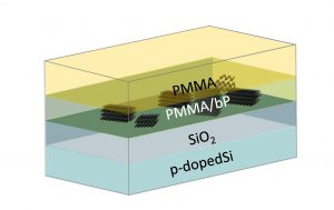
Hybrid materials, containing a 2D filler embedded in a polymeric matrix, are an interesting platform for several applications, because of the variety of properties that the filler can impart to the polymer matrix when dispersed at the nanoscale. Moreover, novel properties could arise from the interaction between the two. Mostly the bulk properties of these materials have been studied so far, especially focusing on how the filler changes the polymeric matrix properties. Here we propose a complete change of perspective by using the hybrid nanocomposite material as a platform suitable to engineer the properties of the filler and to exploit its potential in the fabrication of devices. As a proof of concept of the versatility and the potential of the new method, we applied this approach to prepare black phosphorus nanocomposites through its dispersion in poly (methyl methacrylate). Black phosphorus is a very interesting 2D material, whose application have so far been limited by its high reactivity to oxygen and water. In this respect, we show that electronic-grade black phosphorus flakes, already embedded in a protecting matrix since their exfoliation from the bulk material, are endowed with significantly increased stability and can be further processed into devices without degrading their properties.
Dephasing in strongly anisotropic black phosphorus
Weak localization was observed and determined in a black phosphorus (bP) field-effect transistor 65 nm thick. The weak localization behaviour was found to be in excellent agreement with the Hikami-Larkin-Nagaoka model for fields up to 1 T, from which characteristic scattering lengths could be inferred. The dephasing length L was found to increase linearly with increasing hole density attaining a maximum value of 55 nm. The temperature dependence of L was also investigated and above 1 K, it was found to decrease weaker than the dependence characteristic of electron-electron scattering in the presence of elastic scattering in two dimensions. Rather, the observed power law was found to be close to that observed previously in other quasi-one-dimensional systems such as metallic nanowires and carbon nanotubes. We attribute our result to the crystal structure of bP which host a puckered honeycomb lattice forming a strongly anisotropic medium for localization.