Manipulating quantum Hall edge channels in graphene through Scanning Gate Microscopy
Scanning Gate Microscopy (SGM) employs the biased metallic tip of an Atomic Force Microscope to gate the sample in a region located underneath the tip, with nanometer precision. This modifies the charge carrier concentration in the gated part of the sample. We are able to locally gate a region of choice of a narrow graphene Hall bar in the quantum Hall regime, which allows for the manipulation and deflection of quantum Hall edge channels. By selecting the appropriate parameters, edge channels can be made to interact, equilibrate, and/or backscatter. As a consequence of the gradual spatial variation of the tip potential, which differs significantly from the potential of a more standard top- or split-gate, we see intriguing junctions arise between regions of different charge carrier density, which manifests itself in values of the longitudinal resistance Rxx (see Fig. 1) that have not been observed before in devices based on top- or split-gates. The solution of the corresponding quantum scattering problem substantiates these results.
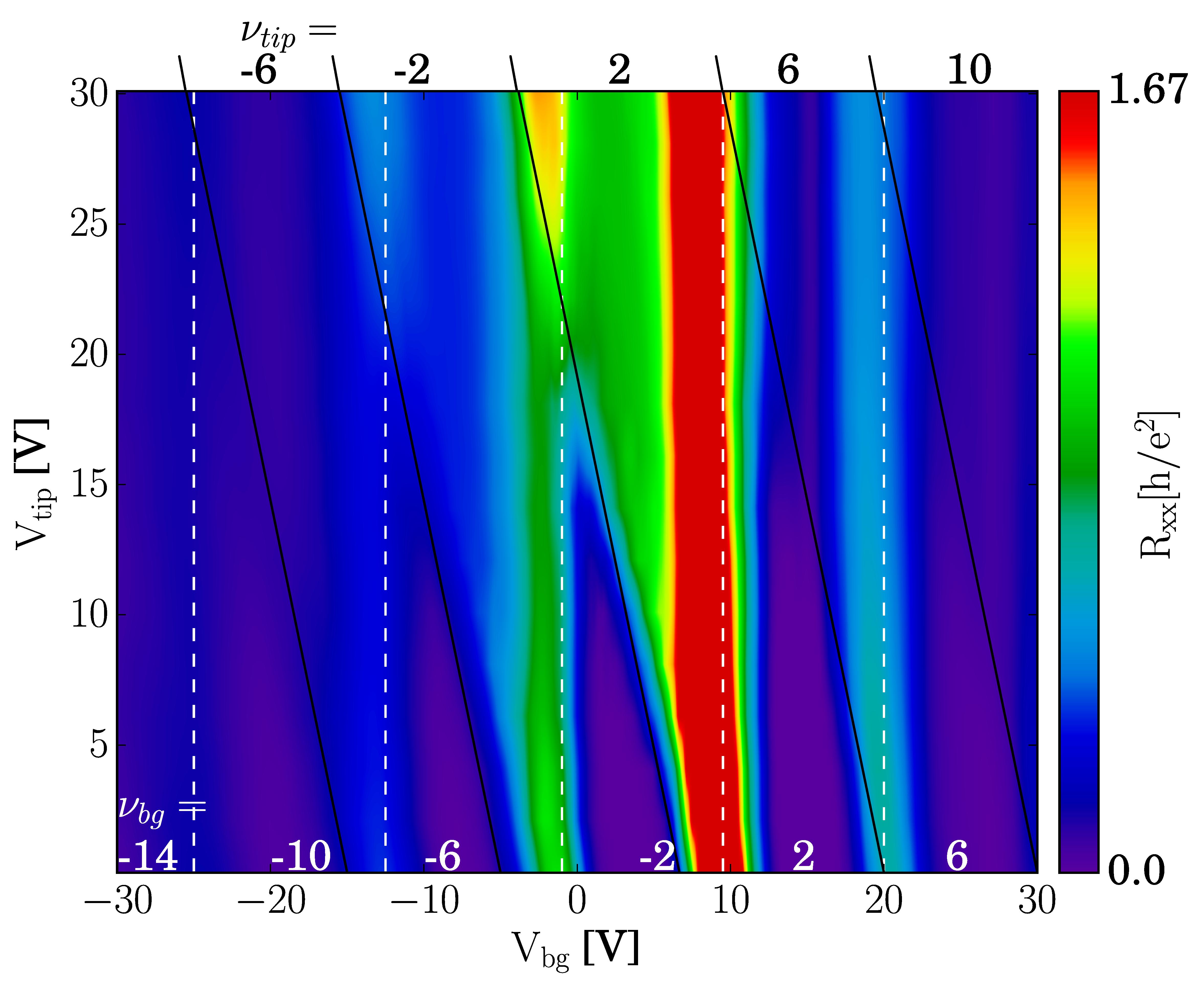
Figure 1: A 2D map, showing the value of Rxx as a function of back gate voltage Vbg and tip voltage Vtip. The data was collected by sweeping the back gate from -30 to +30 V, while increasing the tip bias in steps of 2 V in-between sweeps. The global filling factors vbg and the filling factors underneath the SGM tip vtip are indicated. Magnetic field B = 8 T, temperature T = 4.2 K.
The SGM approach offers several advantages with respect to more conventional solutions with fixed gates. Being able to move the tip freely gives great flexibility in manipulating the edge channels, which can be done by changing the tip position, the tip-sample distance, and the applied voltage. Possible follow-up experiments are in preparation.
Furthermore, we demonstrate theoretically that the phenomenon of current confinement along graphene n-p junctions at high magnetic fields can be used to form an Aharonov-Bohm interferometer. The interference system exploits a closed n-p junction that can be induced by a floating gate within the sample, and coupling of the junction currents with the edge currents in the quantum Hall regime. Operation of the device requires current splitting at the edge and the n-p junction contacts which is found for armchair ribbons at low Fermi energy.
Figure 2 sketches the current distributions in the quantum Hall regime. The Fermi energy is set within the conduction band of the ribbon. The potential of the tip placed above the center of the ribbon raises the valence band top above the Fermi energy, inducing a circular region of p-type conductivity. The current flows near the edge of the ribbon and along the n-p junction. For radius of the n-p junction large enough to approach the edges of the sample, the edge current couples to the n-p junction and flows around the circular p region [Fig. 2(a)]. For a higher Fermi energy, the radius of the n-p junction gets smaller, and the coupling of the edge current to the junction becomes weaker. At some point [Fig. 2(b)] the edge current can no longer couple to the n-p junction.

Figure 2: Schematic drawing of the currents in the system in the quantum Hall regime. (a) Low Fermi energy and edge current coupled to the n-p junction. (b) For high Fermi energy, the radius of the n-p junction decreases, and the junction is too far from the edge for the edge current to couple to the n-p junction.
The oscillation period for a given Fermi energy is similar for both the semiconducting and metallic ribbons [Fig. 3(a)]. We find that the oscillation period can be quite accurately associated with the radius of the n-p junction induced by the tip. The distribution of the current amplitude is plotted in Figs. 3(b)–3(c) for the the magnetic fields marked by points in Fig. 3(a). The circles in Figs. 3(b)–3(c) denote the n-p junction line. Concluding the above findings, formation of a periodic oscillation pattern that is observed in Fig. 3(a) at higher B results from the current confinement at the n-p junction that appears in the quantum Hall regime.
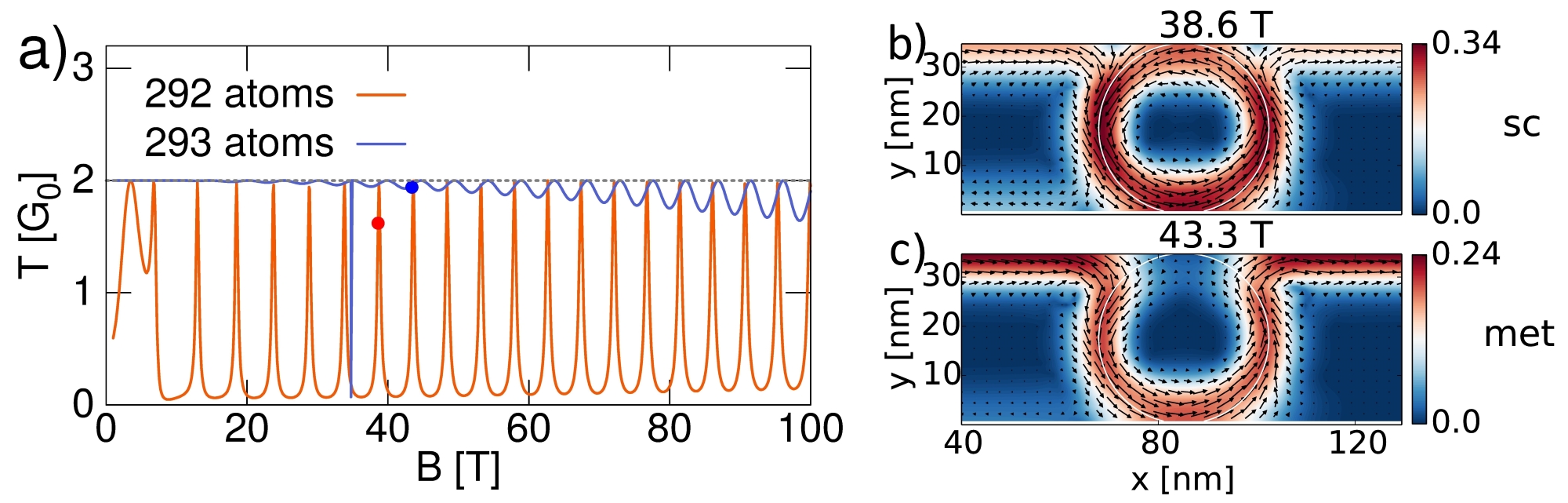 Figure 3: (a) Summed electron transfer probability for armchair nanoribbons [semiconducting with 292 atoms across the channel (35.79 nm)—orange lines, and metallic with 293 atoms across the channel (35.92 nm)—blue lines] in the lowest sub-band transport conditions. The tip is located above the axis of the channel. The applied tip potential is 400 meV, and d = 4.92 nm. In (b)–(c), maps of the square root of the current amplitude are plotted with the orientation of the vector current distribution. Plot (b) was calculated for the semiconducting, and (c) for the metallic ribbon. Plot (b) was made for the semiconducting ribbon—see the orange dot in (a). Plot (c) corresponds to the metallic ribbon and was taken for the magnetic field marked by the blue dot in (a).
Publications:
- A. Mrenca-Kolasinska, S. Heun, and B. Szafran: Aharonov-Bohm interferometer based on n- p junctions in graphene nanoribbons, arXiv:1510.04593 [cond-mat.mes-hall].
- A. Mrenca-Kolasinska, S. Heun, and B. Szafran: Aharonov-Bohm interferometer based on n- p junctions in graphene nanoribbons, Phys. Rev. B 93, 125411 (2016).
- Selected for Phys. Rev. B Kaleidoscope March 2016.
- L. Bours: Edge channel transport in graphene nanoribbons, Master thesis, Radboud University Nijmegen, The Netherlands, 2016.
- Lennart Bours, Stefano Guiducci, Alina Mrenca-Kolasinska, Bartlomiej Szafran, Jan C. Maan, and Stefan Heun: Manipulating quantum Hall edge channels in graphene through Scanning Gate Microscopy, arXiv:1707.02855 [cond-mat.mes-hall].
- L. Bours, S. Guiducci, A. Mrenca-Kolasinska, B. Szafran, J. C. Maan, and S. Heun: Manipulating quantum Hall edge channels in graphene through scanning gate microscopy, Phys. Rev. B 96 (2017) 195423.
- Quantum Hall effect in hybrid Josephson junctions, NEST Scientific Report 2014 – 2020.
Presented at:
- A. Mreńca-Kolasińska, S. Heun, and B. Szafran: Aharonov-Bohm effect along a circular n-p junction in graphene nanoribbon, Graphene Week 2016, Warsaw, Poland, 13 – 17 June 2016 (poster). [Poster]
- A. Mreńca-Kolasińska, S. Heun, and B. Szafran: Gate-induced Aharonov-Bohm interferometer in graphene nanoribbon, 45th “Jaszowiec” International School and Conference on the Physics of Semiconductors, Szczyrk, Poland, 18 – 24 June 2016 (oral). [Program] [Talk]
- L. Bours: Manipulating Edge Channel Transport in Graphene, Master thesis presentation, Radboud University Nijmegen, The Netherlands, 12 September 2016.
- A. Mreńca-Kolasińska, B. Szafran, L. Bours, S. Guiducci, J. C. Maan, and S. Heun: Resonance microscopy of quantum transport in graphene – SGM-induced junctions, PhD Seminar, Radocza, Poland, 25 March 2017. [Talk]
- S. Heun: Quantum Hall Effect in Graphene, Universitaet Osnabrueck, Germany (Prof. J. Wollschlaeger), 30 June 2017 (invited). [Abstract] [Talk]
- S. Heun: The importance of surfaces for the properties of 2D materials: from graphene to phosphorene, University of Seoul, S. Korea (Prof. Jeil Jung), 22 September 2017 (invited). [Abstract] [Talk]
- L. Bours, S. Guiducci, A. Mrenca-Kolasinska, B. Szafran, J. C. Maan, and S. Heun: Manipulating quantum Hall edge channels in graphene by Scanning Gate Microscopy, NSS-9, Gyeongju, S. Korea, 25 – 28 September 2017 (invited). [Abstract] [Talk]
- L. Bours, S. Guiducci, A. Mrenca-Kolasinska, B. Szafran, J. C. Maan, and S. Heun: Manipulating quantum Hall edge channels through Scanning Gate Microscopy, DPG Spring Meeting and EPS-CMD 27, Berlin, Germany, 11 – 16 March 2018 (oral). [Abstract] [Talk]