MBE growth of self-assisted InAs nanowires on graphene
The growth of InAs nanowires for various mesoscopic physics experiments has so far drawn much attention thanks to their unique properties. Namely, their high aspect ratio, high electron mobility, the surface pinning in the conduction band, the large spin orbit coupling and high Lande g-factor. These turn them quite suitable for possible observation of the Majorana fermions among many other experiments. InAs nanowires are most successfully grown by gold assisted VLS growth. Nevertheless, replacing the gold droplet with an indium eliminates the potential risk of gold doping along the nanowires which might act as scattering centers degrading the conductance properties. Self-assisted growth of InAs nanowires on Si/SiO2 has been demonstrated by several groups resulting mostly in low aspect ratio nanowires and a highly twinned zinc blende crystal structure. The mixed structure has been attributed to the lack of a liquid droplet at the top of the nanowire, associated with the lower surface tension of the In metal.
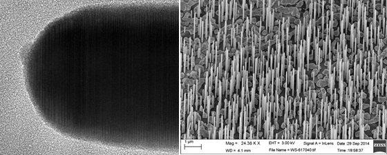 Fig 1: Right: SEM image of InAs nanowires grown on a zero/buffer layer graphene. Left: TEM image of the tip of a single nanowire, showing the mixed crystal structure.
Graphene has recently been shown to provide an intriguing platform for growth of a variety of III-V semiconductor nanowires. Following work at NTNU Norway and by the Fukui group in Japan we pursued the self-assisted growth of InAs nanowires on graphene formed by evaporation of Si from SiC. The growth of nanowires on this type of graphene substrate is significantly more easily obtained as compared to growth on Si/SiO2, thanks to the unique long range lattice matching between InAs and graphene. We studied the effect of the nanowire growth parameters such as nucleation conditions, In flux, group V/III ratio and substrate temperature. In particular, we looked into the properties of the high purity graphene layer, namely, a bilayer, a zero/buffer layer or hydrogen-intercalated graphene. We found that the use of the so called zero layer/ buffer layer rather than a complete graphene layer facilitated the growth of much thinner nanowires. We studied the nanowires distribution and morphology by SEM (Figure 1 right image) and their crystal structure by TEM which occasionally provides evidence for the presence of an indium droplet at the tip of the nanowires (Figure 1 left image). This together with the small diameters we managed to obtain (40-60 nm) was not as yet sufficient to provide self-assisted growth of nanowires having a pure phase. Instead the wires had a typical mixed wurtzite/zincblende structure with semi periodic regions along the growth direction. Conductance measurements on the self-assisted nanowires at low temperature show a similar behavior to our gold assisted ones. The growth of conducting InAs nanowires on a conducting layer such as graphene opens up new possibilities for electronic and electro optic nanowire devices where the substrate can serve as a global contact/gate.
Publications:
- Jung-Hyun Kang, Yuval Ronen, Yonatan Cohen, Domenica Convertino, Antonio Rossi, Camilla Coletti, Stefan Heun, Lucia Sorba, Perla Kacman, and Hadas Shtrikman: MBE growth of self-assisted InAs nanowires on graphene, arXiv:1610.00430 [cond-mat.mtrl-sci].
- Jung-Hyun Kang, Yuval Ronen, Yonatan Cohen, Domenica Convertino, Antonio Rossi, Camilla Coletti, Stefan Heun, Lucia Sorba, Perla Kacman, and Hadas Shtrikman: MBE growth of self-assisted InAs nanowires on graphene, Semicond. Sci. Technol. 31 (2016) 115005.
Featured on Cover Page of Issue 11 of Semicond. Sci. Technol. - U. P. Gomes, D. Ercolani, V. Zannier, S. Battiato, E. Ubyivovk, V. Mikhailovskii, Y. Murata, S. Heun, F. Beltram, and L. Sorba: Heterogeneous nucleation of catalyst-free InAs nanowires on silicon, arXiv:1701.05153 [cond-mat.mes-hall].
- U. P. Gomes, D. Ercolani, V. Zannier, S. Battiato, E. Ubyivovk, V. Mikhailovskii, Y. Murata, S. Heun, F. Beltram, and L. Sorba: Heterogeneous nucleation of catalyst-free InAs nanowires on silicon, Nanotechnology 20 (2017) 065603.
- Semiconductor nanowires: growth mechanisms and dynamics, NEST Scientific Report 2014 – 2020.
Presented at:
- Jung-Hyun Kang, Yonatan Cohen, Yuval Ronen, Moty Heiblum, Domenica Convertino, Vaidotas Miseikis, Camilla Coletti, Stefan Heun, Lucia Sorba, and Hadas Shtrikman: MBE Growth of Self Assisted InAs Nanowires on Graphene, CIMTEC 2016, Perugia, Italy, 5-9 June 2016 (invited). [Abstract] [Talk]
- D. Ercolani, U. P. Gomes, V. Zannier, S. Battiato, E. Ubyivovk, V. Mikhailovskii, Y. Murata, S. Heun, F. Beltram, and L. Sorba: Heterogeneous nucleation of CBE grown catalyst-free InAs nanowires on silicon, 19th European Workshop on Molecular Beam Epitaxy, Korobitsyno, St. Petersburg, Russia, March 19-22, 2017 (poster). [Abstract] [Poster]
- S.Battiato, D. Ercolani, U. P. Gomes, V. Zannier, E. Ubyivovk, V. Mikhailovskii, Y. Murata, S. Heun, F. Beltram, and L. Sorba: Heterogenous nucleation of catalyst-free InAs nanowires on Silicon, 25th Int. Symp. “Nanostructures: Physics and Technology”, Saint Petersburg, Russia, June 26–30, 2017 (oral). [Abstract] [Talk]
- I. Verma, V. Zannier, D. Ercolani, S. Salimian, F. Rossella, S. Heun, and L. Sorba: InSb Nanoflags: Growth and Transport Study, EuroMBE 2019, Lenggries, Germany, February 17th to 20th, 2019 (poster). [Abstract] [Poster]