Low-temperature quantum transport in CVD-grown single crystal graphene
Chemical vapor deposition (CVD) has been proposed for large-scale graphene synthesis for practical applications. However, the inferior electronic properties of CVD graphene are one of the key problems to be solved. Several protocols were reported to improve the electrical characteristics of CVD-graphene, including a dry transfer technique and the use of flakes of hexagonal boron nitride (h-BN) as substrates. Dry transfer can reduce the transfer-related contamination thus minimizing the extrinsic doping of CVD graphene. Furthermore, h-BN substrates can provide atomically-smooth surfaces and small lattice mismatch, which leads to reduced substrate-induced scattering. Unfortunately, owing to the small size of h-BN flakes, this method requires a cumbersome aligned-transfer of graphene, and device dimensions are limited.
We have performed a detailed study on the electronic properties of high-quality single crystal monolayer graphene. The graphene is grown by CVD on copper using a cold-wall reactor and then transferred to Si/SiO2. Our low-temperature magneto-transport data demonstrate that the characteristics of the measured single-crystal CVD graphene samples are superior to those of polycrystalline graphene and have a quality which is comparable to that of exfoliated graphene on Si/SiO2. The Dirac point in our best samples is located at back gate voltages of less than 10 V, and their mobility can reach 11000 cm2/Vs. More than 12 flat and discernible half-integer quantum Hall plateaus have been observed in high magnetic field on both the electron and hole side of the Dirac point (see Fig. 1). At low magnetic field, the magnetoresistance shows a clear weak localization peak. Using the theory of McCann et al., we find that the inelastic scattering length is larger than 1 μm in these samples even at the charge neutrality point, much larger than the results reported in previous studies on CVD graphene.
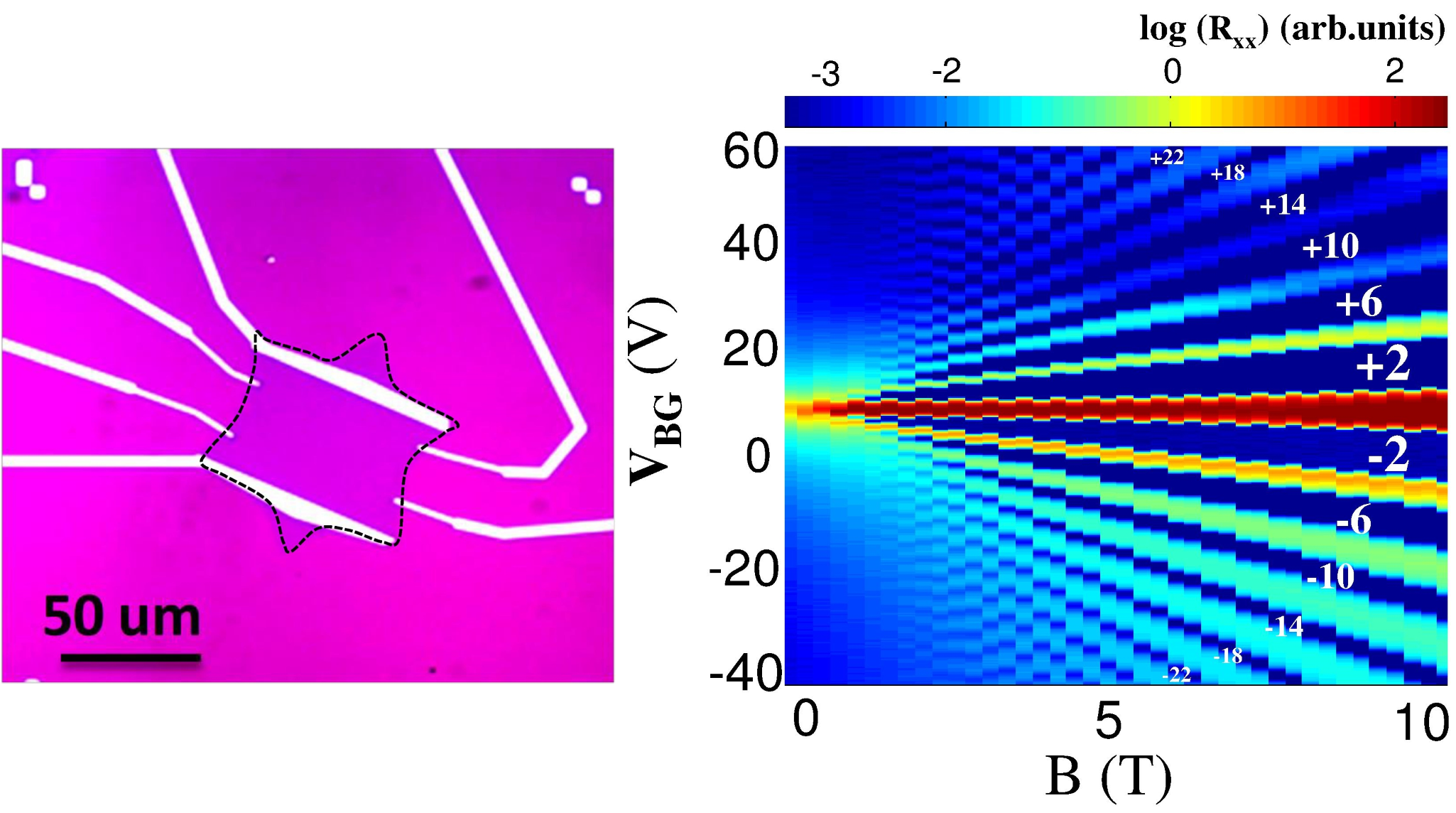
Fig. 1: Left: Optical microscopy image of CVD-graphene device. Right: Landau fan diagram of longitudinal resistance as a function of back gate voltage and magnetic field. There are more than 12 Landau levels clearly observed.
Publications:
- Vaidotas Miseikis, Domenica Convertino, Neeraj Mishra, Mauro Gemmi, Torge Mashoff, Stefan Heun, Niloofar Haghighian, Francesco Bisio, Maurizio Canepa, Vincenzo Piazza, Camilla Coletti: Rapid CVD growth of millimetre-sized single crystal graphene using a cold-wall reactor, arXiv:1501.06356 [cond-mat.mtrl-sci].
- V. Miseikis, D. Convertino, N. Mishra, M. Gemmi, T. Mashoff, S. Heun, N. Haghighian, F. Bisio, M. Canepa, V. Piazza, and C. Coletti: Rapid CVD growth of millimetre-sized single crystal graphene using a cold-wall reactor, 2D Mater. 2 (2015) 014006.
- Luca Planat: Study and characterization of CVD-grown single crystal graphene, Internship Report, May – July 2015.
- S. Xiang, V. Miseikis, L. Planat, S. Guiducci, S. Roddaro, C. Coletti, F. Beltram, and S. Heun: Low-temperature quantum transport in CVD-grown single crystal graphene, arXiv:1603.07499 [cond-mat.mes-hall].
- S. Xiang, V. Miseikis, L. Planat, S. Guiducci, S. Roddaro, C. Coletti, F. Beltram, and S. Heun: Low-temperature quantum transport in CVD-grown single crystal graphene, Nano Research 9, 1823 (2016). [Free Link]
- V. Miseikis, S. Xiang, S. Roddaro, S. Heun, and C. Coletti: Perfecting the growth and transfer of large single-crystal CVD graphene: a platform material for optoelectronic applications, arXiv:1711.05048 [cond-mat.mtrl-sci].
- V. Miseikis, S. Xiang, S. Roddaro, S. Heun, and C. Coletti: Perfecting the growth and transfer of large single-crystal CVD graphene: a platform material for optoelectronic applications, in: GraphITA, selected papers from the workshop, pp. 113 – 124, Editors: V. Morandi and L. Ottaviano, Springer, 2017 (DOI: 10.1007/978-3-319-58134-7_8).
- Stefan Heun, Stefano Roddaro: Low-temperature quantum transport in 2D materials, CNR Nano Activity Report 2018 [Page 52].
- Y. Ogawa, Y. Murata, S. Suzuki, H. Hibino, S. Heun, Y. Taniyasu, and K. Kumakura: Surface structures of graphene covered Cu(103), arXiv:1809.00915 [cond-mat.mtrl-sci].
- Y. Ogawa, Y. Murata, S. Suzuki, H. Hibino, S. Heun, Y. Taniyasu, and K. Kumakura: Surface structures of graphene covered Cu(103), Jpn. J. Appl. Phys. 57 (2018) 100301.
- Scalable high-mobility graphene for photonics and biomedicine, NEST Scientific Report 2014 – 2020.
Presented at:
- V. Mišeikis, D. Convertino, N. Mishra, M. Gemmi, T. Mashoff, S. Heun, N. Haghighian, F. Bisio, M. Canepa, V. Piazza and C. Coletti: Rapid CVD growth of millimetre-sized single-crystal graphene using a cold-wall reactor, Graphene 2015, Bilbao, Spain, March 10-13, 2015 (oral). [Abstract] [Talk]
- S. Xiang, V. Miseikis, L. Planat, S. Guiducci, S. Roddaro, C. Coletti, F. Beltram, and S. Heun: Low-temperature quantum transport in CVD-grown single crystal graphene, Nanosea 2016, Giardini Naxos (ME), Italy, July 3rd-8th, 2016 (oral). [Abstract] [Talk]
- S. Xiang, V. Miseikis, L. Planat, S. Guiducci, S. Roddaro, C. Coletti, F. Beltram, and S. Heun: Low-temperature quantum transport in CVD-grown single crystal graphene, 33rd International Conference on the Physics of Semiconductors (ICPS), Beijing, China, July 31 – August 5, 2016 (poster). [Abstract] [Poster]
- Y. Ogawa, Y. Murata, S. Suzuki, H. Hibino, S. Heun, and K. Kumakura: Single-layer graphene grown on Cu{120} plane by chemical vapor deposition method, Japanese Society of Applied Physics Autumn Meeting, Toki Messe Niigata City, Japan, September 13 – 16, 2016 (oral). [Abstract] [Talk]
- S. Guiducci: Low-temperature quantum transport in CVD-grown single crystal graphene, Progress Meeting Fondazione Silvio Tronchetti Provera, Pisa, Italy, 6 October 2016 (oral). [Talk]
- Y. Ogawa, Y. Murata, S. Suzuki, H. Hibino, S. Heun, and K. Kumakura: Surface morphology changes of CVD-graphene/Cu{120} induced by post-annealing processes, The 30th International Microprocesses and Nanotechnology Conference (MNC 2017), Ramada Plaza JeJu Hotel, JeJu, Korea, November 6 – 9, 2017 (poster). [Abstract] [Poster]