Half-integer Shapiro steps in highly transmissive InSb nanoflag Josephson junctions
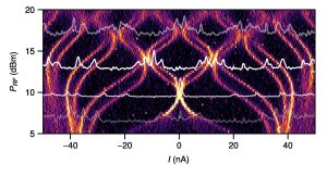
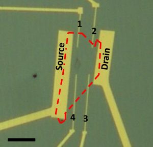
We investigate a ballistic InSb nanoflag-based Josephson junction with Nb superconducting contacts. The high transparency of the superconductor-semiconductor interfaces enables the exploration of quantum transport with parallel short and long conducting channels. Under microwave irradiation, we observe half-integer Shapiro steps that are robust to temperature, suggesting their possible nonequilibrium origin. Our results demonstrate the potential of ballistic InSb nanoflags Josephson junctions as a valuable platform for understanding the physics of hybrid devices and investigating their nonequilibrium dynamics.
Josephson Diode Effect in High Mobility InSb Nanoflags
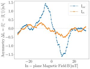
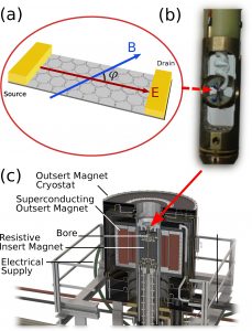
We report evidence of non-reciprocal dissipation-less transport in single ballistic InSb nanoflag Josephson junctions, owing to a strong spin-orbit coupling. Applying an in-plane magnetic field, we observe an inequality in supercurrent for the two opposite current propagation directions. This demonstrates that these devices can work as Josephson diodes, with dissipation-less current flowing in only one direction. For small fields, the supercurrent asymmetry increases linearly with the external field, then it saturates as the Zeeman energy becomes relevant, before it finally decreases to zero at higher fields. We show that the effect is maximum when the in-plane field is perpendicular to the current vector, which identifies Rashba spin-orbit coupling as the main symmetry-breaking mechanism. While a variation in carrier concentration in these high-quality InSb nanoflags does not significantly influence the diode effect, it is instead strongly suppressed by an increase in temperature. Our experimental findings are consistent with a model for ballistic short junctions and show that the diode effect is intrinsic to this material. Our results establish InSb Josephson diodes as a useful element in superconducting electronics.
Toward Quantum Hall Effect in a Josephson Junction
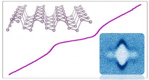
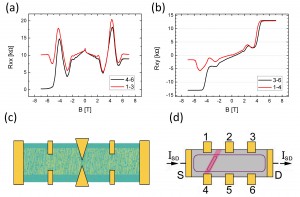
Hybrid superconductor/semiconductor devices constitute a powerful platform where intriguing topological properties can be investigated. We present fabrication methods and analysis of Josephson junctions formed by a high-mobility InAs quantum-well bridging two Nb superconducting contacts. We demonstrate supercurrent flow with transport measurements, critical temperature of 8.1 K, and critical fields of the order of 3 T. Modulation of supercurrent amplitude can be achieved by acting on two side gates lithographed close to the two-dimensional electron gas. Low-temperature measurements reveal also well-developed quantum Hall plateaus, showing clean quantization of Hall conductance. Here, the side gates can be used to manipulate channel width and electron carrier density in the device. These findings demonstrate the potential of these hybrid devices to investigate the coexistence of superconductivity and Quantum Hall effect and constitute the first step in the development of new device architectures hosting topological states of matter.
Black Phosphorus Planar Josephson Junctions
Setting up strong Josephson coupling in van der Waals materials in close proximity to superconductors offers several opportunities both to inspect fundamental physics and to develop cryogenic quantum technologies. Here we show evidence of Josephson coupling in a planar few-layer black Phosphorus junction. The planar geometry allows to probe the junction behavior by means of external gates, at different carrier concentrations. Clear signatures of Josephson coupling are demonstrated by measuring supercurrent flow through the junction at milli-Kelvin temperatures. Manifestation of Fraunhofer pattern with a transverse magnetic field is also observed, confirming the Josephson coupling. These findings represent evidence of proximity Josephson coupling in a planar junction based on a van der Waals material beyond graphene and will expedite further studies, exploiting the peculiar properties of exfoliated black phosphorus thin flakes.
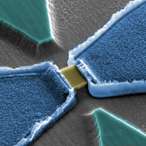
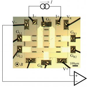
High Mobility Free-Standing InSb Nanoflags for Advanced Quantum Technologies

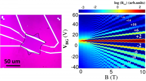
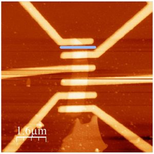
High-quality III-V narrow band-gap semiconductor materials with strong spin-orbit coupling and large Landé g-factor provide a promising platform for next-generation applications in the field of optoelectronics, spintronics, and quantum computing. Indium antimonide (InSb) offers a narrow band gap, high carrier mobility, and a small effective mass, and thus perfectly fits to this scope. In fact, it has attracted tremendous attention in recent years for the implementation of topological superconducting states supporting Majorana zero modes. However, high quality heteroepitaxial two-dimensional (2D) InSb layers are very difficult to realize owing to the large lattice mismatch with other widespread semiconductor substrates. A solution to this problem is to grow free-standing single-crystalline 2D InSb nanostructures, so-called nanoflags. We have performed a thorough low-temperature magneto-transport characterization of InSb nanoflag-based Hall-bar and Josephson junction devices. We demonstrate high electron mobility (~29,000 cm2/Vs) and significant supercurrent (~50 nA at 300 mK), which places InSb nanoflags in the spotlight as a versatile and convenient 2D platform for advanced quantum technologies.
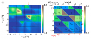
Programmable quantum Hall bisector: towards a novel resistance standard for quantum metrology
We demonstrate a programmable quantum Hall circuit that implements a novel iterative voltage bisection scheme and allows obtaining any binary fraction (k/2n) of the fundamental resistance quantum. The circuit requires a number n of bisection stages that only scales logarithmically with the precision of the fraction. The value of k can be set to any integer between 1 and 2n by proper gate configuration. The architecture exploits gate-controlled routing, mixing, and equilibration of edge modes of robust quantum Hall states. The device does not contain any internal Ohmic contact potentially leading to spurious voltage drops. Our scheme addresses key critical aspects of quantum Hall arrays of resistance standards. The approach is demonstrated in a proof-of-principle two-stage bisection circuit built on a high-mobility GaAs/AlGaAs heterostructure operating at temperature of 260 mK and magnetic field of 4.1 T.
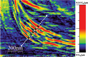
Imaging Fractional Incompressible Stripes in Integer Quantum Hall Systems
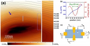
Transport experiments provide conflicting evidence on the possible existence of fractional order within integer quantum Hall systems. In fact, integer edge states sometimes behave as monolithic objects with no inner structure, while other experiments clearly highlight the role of fractional substructures. Recently developed low-temperature scanning probe techniques offer today an opportunity for a deeper-than-ever investigation of spatial features of such edge systems. Here we use scanning-gate microscopy and demonstrate that fractional features were unambiguously observed in every integer quantum Hall constriction studied. We present also an experimental estimate of the width of the fractional incompressible stripes corresponding to filling factors 1/3, 2/5, 3/5, and 2/3. Our results compare well with predictions of the edge-reconstruction theory.
Interedge backscattering in buried split-gate-defined graphene quantum point contacts
Quantum Hall effects offer a formidable playground for the investigation of quantum transport phenomena. Edge modes can be deflected, branched, and mixed by designing a suitable potential landscape in a twodimensional conducting system subject to a strong magnetic field. We demonstrate a buried split-gate architecture and use it to control electron conduction in large-scale single-crystal monolayer graphene grown by chemical vapor deposition. The control of the edge trajectories is demonstrated by the observation of various fractional quantum resistances, as a result of a controllable interedge scattering. Experimental data are successfully modeled both numerically and analytically within the Landauer-Buttiker formalism. Our architecture is particularly promising and unique in view of the investigation of quantum transport via scanning probe microscopy, since graphene constitutes the topmost layer of the device. For this reason, it can be approached and perturbed by a scanning probe down to the limit of mechanical contact.
Manipulating quantum Hall edge channels in graphene through Scanning Gate Microscopy
We show evidence of the backscattering of quantum Hall edge channels in a narrow graphene Hall bar, induced by the gating effect of the conducting tip of a Scanning Gate Microscope, which we can position with nanometer precision. Moreover, we see intriguing junctions arise between regions of different charge carrier density, due to the gradual spatial variation of the gating potential, which manifests itself in values of the longitudinal resistance Rxx that have not been observed before in devices based on top- or split-gates.
Low-temperature quantum transport in CVD-grown single crystal graphene
Chemical vapor deposition (CVD) is typically used for large-scale graphene synthesis for practical applications. However, the inferior electronic properties of CVD graphene are one of the key problems to be solved. Therefore, we present a detailed study on the electronic properties of high-quality single-crystal monolayer graphene. The graphene is grown via CVD on copper, by using a cold-wall reactor, and then transferred to Si/SiO2. Our low-temperature magneto-transport data demonstrate that the characteristics of the single-crystal CVD graphene samples are superior to those of polycrystalline graphene and have a quality which is comparable to that of exfoliated graphene on Si/SiO2. The Dirac point in our best samples occurs at back-gate voltages lower than 10 V, and a maximum mobility of 11,000 cm2/(V·s) is attained. More than 12 flat and discernible half-integer quantum Hall plateaus occur under a high magnetic field on both the electron and hole sides of the Dirac point. At a low magnetic field, the magnetoresistance exhibits a weak localization peak. Using the theory of McCann et al., we obtain inelastic scattering lengths of >1 μm, even at the charge neutrality point of the samples.
Morphology and Magneto-Transport in Exfoliated Graphene on Ultrathin Crystalline β-Si3N4(0001)/Si(111)
We report the first experimental study of graphene transferred on β-Si3N4(0001)/Si(111). A comprehensive quantitative understanding of the physics of ultrathin Si3N4 as a gate dielectric for graphene-based devices is provided. The Si3N4 film is grown on Si(111) under ultra-high vacuum (UHV) conditions and investigated by scanning tunneling microscopy (STM). Subsequently, a graphene flake is deposited on top of it by a polymer-based transfer technique, and a Hall bar device is fabricated from the graphene flake. STM is employed again to study the graphene flake under UHV conditions after device fabrication and shows that the surface quality is preserved. Electrical transport measurements, carried out at low temperature in magnetic field, reveal back gate modulation of carrier density in the graphene channel and show the occurrence of weak localization. Under these experimental conditions, no leakage current between back gate and graphene channel is detected.
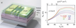
Ohmic contact engineering in few-layer black Phosphorus field effect transistors
Achieving good quality Ohmic contacts to van der Waals materials is a challenge, since at the interface between metal and van der Waals material different conditions can occur, ranging from the presence of a large energy barrier between the two materials to the metallization of the layered material below the contacts. In black phosphorus (bP), a further challenge is its high reactivity to oxygen and moisture, since the presence of uncontrolled oxidation can substantially change the behavior of the contacts. Here we study three of the most commonly used metals as contacts to bP, chromium, titanium, and nickel, and investigate their influence on contact resistance against the variability between different flakes and different samples. Using the transfer length method, from an analysis of ten devices, both at room temperature and at low temperature, Ni results to provide the lowest contact resistance to bP and minimum scattering between different devices. Moreover, we observe that our best devices approach the quantum limit for contact resistance both for Ni and for Ti contacts.
Non-Classical Longitudinal Magneto-Resistance in Anisotropic Black Phosphorus
Resistivity measurements of a few-layer black phosphorus (bP) crystal in parallel magnetic fields up to 45 T are reported as a function of the angle between the in-plane field and the source-drain (S-D) axis of the device. The crystallographic directions of the bP crystal were determined by Raman spectroscopy, with the zigzag axis found within 5 deg of the S-D axis, and the armchair axis in the orthogonal planar direction. A transverse magneto-resistance (TMR) as well as a classically-forbidden longitudinal magneto-resistance (LMR) are observed. Both are found to be strongly anisotropic and non-monotonic with increasing in-plane field. Surprisingly, the relative magnitude (in %) of the positive LMR is larger than the TMR above 32 T. Considering the known anisotropy of bP whose zigzag and armchair effective masses differ by a factor of approximately seven, our experiment strongly suggests this LMR to be a consequence of the anisotropic Fermi surface of bP, as proposed theoretically in the context of three-dimensional structures [Pal and Maslov, Phys. Rev. B81, 214438 (2010)].
Hybrid Nanocomposites of 2D Black Phosphorus Nanosheets Encapsulated in PMMA Polymer Material: New Platforms for Advanced Device Fabrication
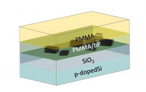
Hybrid materials, containing a 2D filler embedded in a polymeric matrix, are an interesting platform for several applications, because of the variety of properties that the filler can impart to the polymer matrix when dispersed at the nanoscale. Moreover, novel properties could arise from the interaction between the two. Mostly the bulk properties of these materials have been studied so far, especially focusing on how the filler changes the polymeric matrix properties. Here we propose a complete change of perspective by using the hybrid nanocomposite material as a platform suitable to engineer the properties of the filler and to exploit its potential in the fabrication of devices. As a proof of concept of the versatility and the potential of the new method, we applied this approach to prepare black phosphorus nanocomposites through its dispersion in poly (methyl methacrylate). Black phosphorus is a very interesting 2D material, whose application have so far been limited by its high reactivity to oxygen and water. In this respect, we show that electronic-grade black phosphorus flakes, already embedded in a protecting matrix since their exfoliation from the bulk material, are endowed with significantly increased stability and can be further processed into devices without degrading their properties.
Correlation between morphology and transport properties of quasi-free-standing monolayer graphene
We investigate the morphology of quasi-free-standing monolayer graphene (QFMLG) formed at several temperatures by hydrogen intercalation and discuss its relationship with transport properties. Features corresponding to incomplete hydrogen intercalation at the graphene-substrate interface are observed by scanning tunneling microscopy on QFMLG formed at 600 and 800C. They contribute to carrier scattering as charged impurities. Voids in the SiC substrate and wrinkling of graphene appear at 1000C, and they decrease the carrier mobility significantly.
Dephasing in strongly anisotropic black phosphorus
Weak localization was observed and determined in a black phosphorus (bP) field-effect transistor 65 nm thick. The weak localization behaviour was found to be in excellent agreement with the Hikami-Larkin-Nagaoka model for fields up to 1 T, from which characteristic scattering lengths could be inferred. The dephasing length L was found to increase linearly with increasing hole density attaining a maximum value of 55 nm. The temperature dependence of L was also investigated and above 1 K, it was found to decrease weaker than the dependence characteristic of electron-electron scattering in the presence of elastic scattering in two dimensions. Rather, the observed power law was found to be close to that observed previously in other quasi-one-dimensional systems such as metallic nanowires and carbon nanotubes. We attribute our result to the crystal structure of bP which host a puckered honeycomb lattice forming a strongly anisotropic medium for localization.
Scanning Gate Imaging of the 0.7 anomaly
The origin of the anomalous transport feature appearing at a conductance G ≈ 0.7 × (2e2/h) in quasi-1D ballistic devices–the so-called 0.7 anomaly–represents a long standing puzzle. Several mechanisms have been proposed to explain it, but a general consensus has not been achieved. Proposed explanations have been based on quantum interference, the Kondo effect, Wigner crystallization, and other phenomena. A key open issue is whether the point defects that can occur in these low-dimensional devices are the physical cause behind this conductance anomaly. Here we adopt a scanning gate microscopy technique to map individual impurity positions in several quasi-1D constrictions and correlate these with conductance characteristics. Our data demonstrate that the 0.7 anomaly can be observed irrespective of the presence of localized defects, and we conclude that the 0.7 anomaly is a fundamental property of low-dimensional systems.
Bilayer-induced asymmetric quantum Hall effect in epitaxial graphene
The transport properties of epitaxial graphene on SiC(0001) at quantizing magnetic fields are investigated. Devices patterned perpendicularly to SiC terraces exhibit bilayer inclusions distributed along the substrate step edges. The transport properties in the quantum Hall regime are heavily affected by the presence of bilayer inclusions, and observe a significant departure from the conventional quantum Hall characteristics. We observe anomalous values of the quantized resistance and a peculiar asymmetry with magnetic field which was not observed before for graphene on SiC. A quantitative model involving enhanced inter-channel scattering mediated by the presence of bilayer inclusions is presented that successfully explains the observed symmetry properties.
Tuning of quantum interference in top gated graphene
We report on quantum-interference measurements in top-gated Hall bars of monolayer graphene epitaxially grown on the Si face of SiC, in which the transition from negative to positive magnetoresistance was achieved varying temperature and charge density. We perform a systematic study of the quantum corrections to the magnetoresistance due to quantum interference of quasiparticles and electron-electron interaction. We analyze the contribution of the different scattering mechanisms affecting the magnetotransport in the −2.0 × 10^10 cm−2 to 3.75 × 10^11 cm−2 density region and find a significant influence of the charge density on the intravalley scattering time. Furthermore, we observe a modulation of the electron-electron interaction with charge density not accounted for by present theory. Our results clarify the role of quantum transport in SiC-based devices, which
will be relevant in the development of a graphene-based technology for coherent electronics.
Imaging backscattering through impurity-induced antidots in quantum Hall constrictions
We exploit the biased tip of a scanning gate microscope to induce a controlled backscattering between counterpropagating edge channels in a wide constriction in the quantum Hall regime. We compare our detailed conductance maps with a numerical percolation model and demonstrate that conductance fluctuations observed in these devices as a function of the gate voltage originate from backscattering events mediated by localized states pinned by potential fluctuations. Our imaging technique allows us to identify the necessary conditions for the activation of these backscattering processes and also to reconstruct the constriction confinement potential profile and the underlying disorder.
Spectral analysis of inter-channel scattering in the quantum Hall regime by scanning gate microscopy
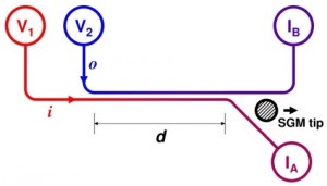
When two separately contacted quantum Hall (QH) edge channels are brought into interaction, they can equilibrate their imbalance via scattering processes. In this work, we use a tunable QH circuit to implement a junction between copropagating edge channels, the length of which can be controlled with continuity. Such a variable device allows us to investigate how current-voltage characteristics evolve when the junction length d is changed. Recent experiments with fixed geometry reported a significant reduction of the threshold voltage for the onset of photon emission, the origin of which is still under debate. Our spatially resolved measurements reveal that this threshold shift depends on the junction length.We discuss this unexpected result on the basis of a model that demonstrates that a heating of electrons is the dominant process responsible for the observed reduction of the threshold voltage.
Equilibration of integer quantum Hall edge channels
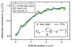
We demonstrate an innovative quantum Hall circuit with variable geometry employing the movable electrostatic potential induced by a biased atomic force microscope tip.We exploit this additional degree of freedom to identify the microscopic mechanisms that allow two co-propagating edge channels to equilibrate their charge imbalance. Experimental results are compared with tight-binding simulations based on a realistic model for the disorder potential. This work provides also an experimental realization of a beam mixer between co-propagating edge channels, a still elusive building block of a recently proposed new class of quantum interferometers.
Selective control of edge channel trajectories by SGM
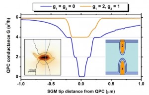
Electronic Mach–Zehnder interferometers in the quantum Hall (QH) regime are currently discussed for the realization of quantum information schemes. A recently proposed device architecture employs interference between two co-propagating edge channels. Here we demonstrate the precise control of individual edge-channel trajectories in quantum point contact devices in the QH regime. The biased tip of an atomic force microscope is used as a moveable local gate to pilot individual edge channels. Our results are discussed in light of the implementation of multi-edge interferometers.
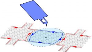
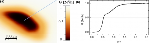
The Scanning Gate Microscopy Laboratory at NEST
The new Scanning Gate Microscopy (SGM) laboratory at NEST is aimed at combining our experience of the transport properties of nanostructures with the opportunity of investigation offered by scanning probe microscopy operating at ultra-low temperature (300mK), in a magnetic field tunable up to 9T. The recently installed instrument allows to locally apply an electric potential by means of the conductive tip of an atomic force microscope (AFM) operating in non-contact mode. This has a number of important applications: for instance we were able to image the coherent flow of electrons across a quantum point contact by measuring the change in the conductance corresponding to the local depletion of the 2DEG underneath the tip.